
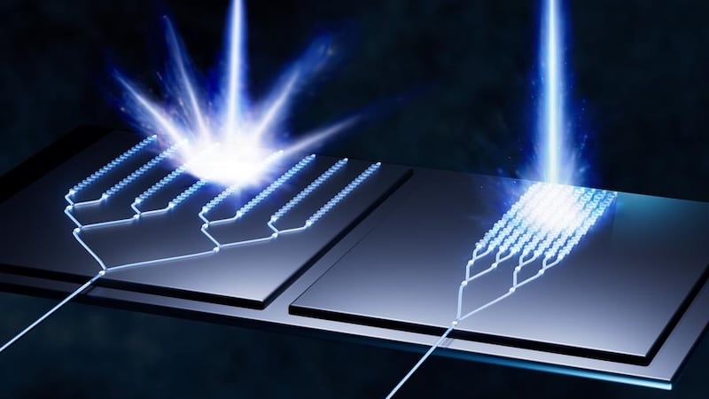
Recent advances in photonics may boost the performance of LiDAR sensors, increase the resolution of image projection, and integrate energy harvesting and light emission into a single display.
Optical computing has not been left out of the recent surge in technological innovation. Scientists are using phase changes for beam steering, compression, image processing, and beyond. The following roundup summarizes recent optical research from the Massachusetts Institute of Technology (MIT), the University of California, Los Angeles (UCLA), and the Institute of Science Tokyo (Science Tokyo).
MIT: A Breakthrough in Optical Light Steering
Researchers at MIT recently published a study outlining a new way to optically steer light. The new technique, utilizing wide-field-of-view (FOV) integrated optical phased arrays (OPAs), could lead to more effective LiDAR sensors that operate without moving parts.
OPAs are typically built on a CMOS-compatible process, with the waveguides constructed using silicon-on-insulator technology. An external laser energizes paths in the silicon, and the path is split several times. The split paths feed into a series of phase-based optical waveguides. The standard OPA separates the waveguides by a full laser wavelength. The new MIT demonstration reduces the waveguide-to-waveguide spacing to ½ wavelength.
Conventional full-wavelength optical waveguide with a limited field of view (left) and a half-wavelength wide-field-of-view waveguide (right). Image used courtesy of MIT
According to the MIT paper, dynamic coupling at a full-wavelength antenna-array spacing generates crosstalk (referred to as grating lobes) starting at ±30 degrees off-center. This gives an effective maximum field of view of 60 degrees. By narrowing the array spacing to ½ wavelength, the lasers coming from each waveguide don’t see each other and don’t interfere. This means the grating lobes don’t appear until ±90 degrees off-center, yielding a theoretical 180-degree field of view.
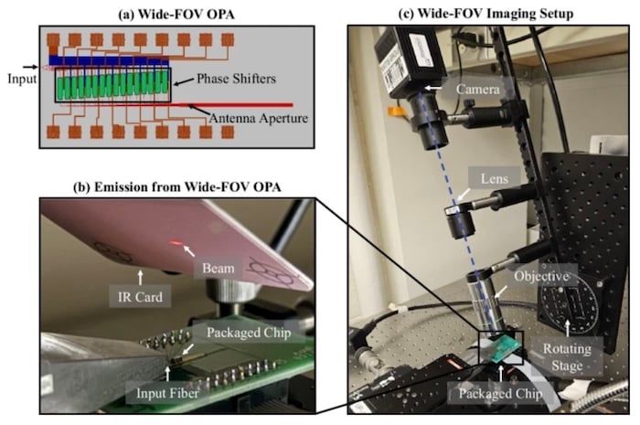
Schematic of a wide-FOV integrated OPA (a), the wide-FOV integrated OPA emitting a single beam onto an infrared-detecting card (b), and the experimental setup with a rotating microscope stage used to obtain the wide-FOV far-field emission profiles of the fabricated chip (c). Image used courtesy of Nature
Their experiment confirmed the ability to position the OPA output across 180 degrees without grating lobes. Multiple tests involved different phase changes with an experimental optical steering range of 15 degrees. The expanded FOV holds the promise for more accurate, less expensive non-mechanical LiDAR systems for automotive and artificial vision applications. The researchers hope to continue tuning the material so that a single chip can steer through the entire 180-degree FOV.
UCLA: Optical Processing for High Depth-of-Field Projection
A group at the UCLA Samueli School of Electrical and Computer Engineering recently demonstrated a high-resolution, extended-depth-of-field projection system. The hybrid optical passive system outlined in their paper utilizes an optical convolutional neural network for 36x phase-based optical data compression.
Space-bandwidth product (SBP) is a measure of the information-carrying capacity of an optical system. Pixel resolution and pixel color depth are the two most familiar components of SBP, but other factors exist as well. Light-wave phase can also be used for information transmission. The UCLA device uses phase encoding to create a lower-resolution image that requires 36x less conventional bandwidth but maintains the same overall SBP as the full-resolution image.
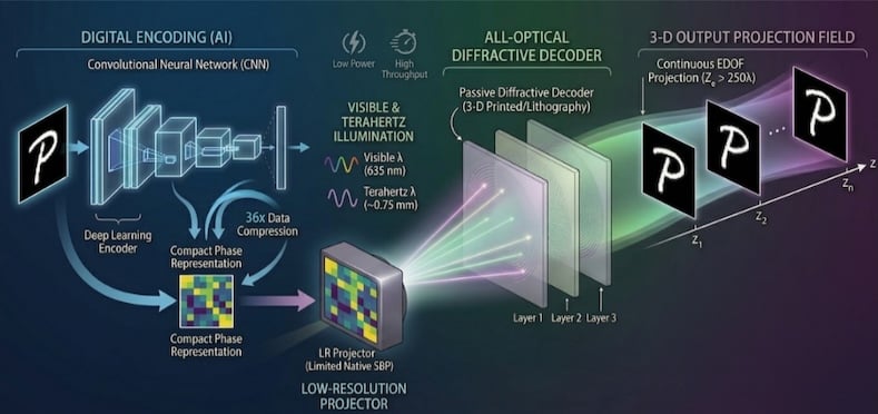
Optical compression and decompression system for extended depth-of-field image projection. Image used courtesy of UCLA
Decoding starts with a low-resolution phase projector (matching the compressed image). The image then passes through a three-part optical diffraction decoder. The decoder decompresses the phase-compressed image and creates a three-dimensional projection with greater depth of field than a conventional projector.
One promising application is close-in augmented reality/virtual reality (AR/VR) technology. The difficulty in focusing on the eye with a conventional close-in projector leads to eye strain and fatigue. The UCLA researchers believe this new system will be able to perform the close-in projection with significantly less user discomfort.
Science Tokyo: Emitting and Generating in the Same Diode
Many semiconductors exhibit some level of the photoelectric effect, including light-emitting diodes (LEDs). However, the effect is generally not strong enough in organic light-emitting diodes (OLEDs)—those common in many small device displays today—to be of practical use for generating electricity.
A research team at the Institute of Science Tokyo (Science Tokyo) recently published a paper describing an OLED structure that shows promise for use as both a display and an energy harvester. Such a device would reduce parts count and device cost by allowing the display semiconductor to also harvest light energy to augment the device’s charging system.

A material structure that operates both as a display and a photovoltaic device. Image used courtesy of Science Tokyo
The photovoltaic effect generates mobile electrons across a semiconductor p-n junction. When an electron moves without another taking its place, it leaves a positively charged space known as a hole. If the electron and hole recombine, either electricity or light is produced. However, visible-light organic semiconductors (as used in OLEDs) exhibit a phenomenon called non-radiative recombination (NRR). When the electron and hole recombine in an OLED, NRR suppresses the generation of electricity, reduces light-generation efficiency, and produces waste heat.
The team’s solution consists of two distinct multi-resonance thermally activated delayed fluorescence (MR-TADF) materials. The team utilized the boron-based v-DABNA and the carbonyl/amine-based QAO in a layered structure. The resulting prototype achieved 1.36% power conversion efficiency and 2% light-emission efficiency. This is the first time an organic semiconductor has exceeded 1% in both properties.
The experimental materials emitted red light at a luminance of 1,000 cd/m2, comparable to current OLED devices. With further work, the team expects the technology to be developed with full color and a practical energy-harvesting level of photovoltaic response.
Trending Products
