
Two new CoolGaN BDS additions replace back-to-back silicon MOSFET pairs with chip-scale packages.
Recently, Infineon Technologies announced the expansion of its CoolGaN BDS 40 V G3 bidirectional switch (BDS) family with two new devices, the IGK048B041S and IGK120B041S. Designed to replace two back-to-back silicon MOSFETs with a single GaN device, the new BDS solutions are said to reduce PCB footprint by up to 82 percent and cut component count in half relative to equivalent discrete MOSFET implementations.
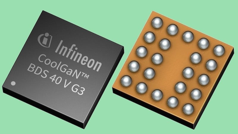
Infineon’s GoolGaN BDS 40 V G3 MOSFET
IGK048B041S and IGK120B041S
According to Infineon, their two new 40 V switching devices are meant to offer a smaller-area design option for bidirectional applications. Rather than bidirectional implementations based on two discrete, back-to-back silicon MOSFETs, the BDS family solutions integrate two GaN devices in a drain-to-drain configuration. To this end, Infineon designed both devices to accept a standard 5 V gate-drive signal, meaning engineers can reuse their existing gate-drive circuits without changing the hardware.
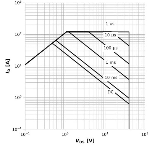
Safe operating area for the IGK048B041S
Within the family, the IGK048B041S comes in a WLCSP chip-scale package measuring 2.1 x 2.1 mm2. At a gate-drain voltage of 5 V and drain current of 5 A, the device posts an RDD(on) of 4.2 mΩ and handles up to 53 A of continuous drain current with pulsed current support up to 120 A.
For designers seeking the smallest portable form factors, the IGK120B041S extends the benefits of its family member into a 1.7 x 1.2 mm2 package at 9 mΩ RDD(on). This smaller device comes with slightly lesser power specifications, including continuous and pulsed drain currents of 30 and 59 A, respectively. More information is available in the data sheets for the IGK048B041S and IGK120B041S.
Bidirectional Blocking and GaN Leakage Advantages
While silicon MOSFETs are ideal for many power applications, they particularly struggle in applications that require bidirectional switching. Namely, every silicon MOSFET contains a parasitic body diode that is an inherent feature of the device’s p-n junction. This diode conducts small amounts of current in the reverse direction during recovery, which can create unwanted conduction fault paths.
To solve this challenge, engineers working around the body diode typically stack two MOSFETs source-to-source in a back-to-back configuration, relying on the opposing body diodes to block in each direction alternately. That approach works, but it doubles the component count and roughly doubles the board area consumed. The series connection also places the on-resistance of two devices in the conduction path.
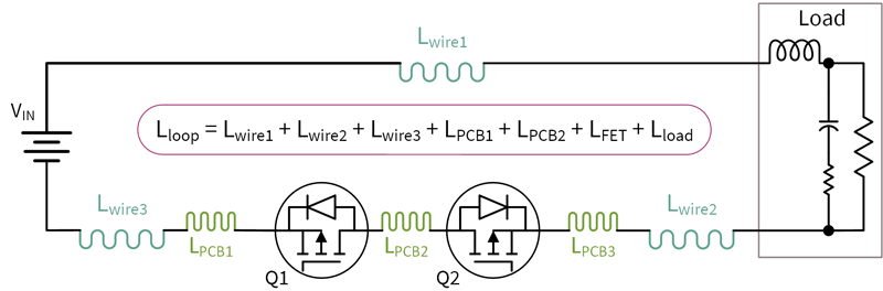
Silicon MOSFETs implemented as bidirectional switches
GaN transistors eliminate the body diode problem at the material level. Enhancement-mode GaN devices are lateral structures built on a two-dimensional electron gas (2DEG) channel, and they carry no parasitic p-n junction between drain and source. When the gate is held below threshold, a GaN switch blocks current in both directions without additional external components.
This true bidirectional blocking capability allows engineers to replace the two-MOSFET stack with a single device in a drain-to-drain configuration, cutting component count and board area while maintaining blocking performance in both directions.
GaN also delivers switching and leakage advantages that matter in portable and fast-charging applications. Gate charge determines how much energy the driver must deliver per cycle and how quickly the device transitions between states, making it the main switching figure of merit in high-frequency designs.
GaN devices post substantially lower gate charge than silicon MOSFETs at equivalent on-resistance, which translates directly into faster switching transitions and lower switching losses per cycle. On leakage, GaN’s wide bandgap suppresses thermally generated carriers far more effectively than silicon, yielding drain-source leakage currents orders of magnitude below what a comparably rated silicon MOSFET produces.
Availability and Family Coverage
With the IGK048B041S and IGK120B041S joining the previously released IGK080B041S, the CoolGaN BDS 40 V G3 family now offers three on-resistance options from 4.2 to 9 mΩ. Both new devices are available now through Infineon’s authorized distribution channels.
All images used courtesy of Infineon.
Trending Products
